Pattern
Deposit a noble-metal catalyst such as Au, Pt, or Ag in the desired geometry.
A semiconductor nanomanufacturing platform
Metal-assisted chemical etching (MacEtch) uses a patterned catalyst to localize redox chemistry at a semiconductor interface—translating a metal pattern into deep, anisotropic micro- and nanostructures without plasma-induced lattice damage.
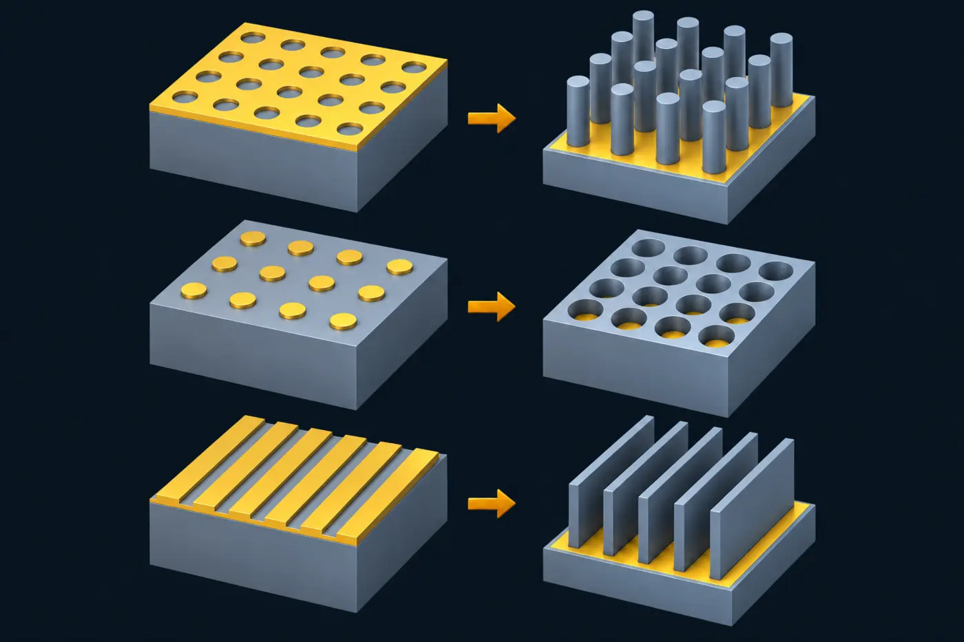
The catalyst geometry determines whether MacEtch produces pillars, holes, or sheets while preserving high anisotropy.
Mechanism
The catalyst does more than mask the surface. It defines where charge transfer—and therefore material removal—can proceed.
Deposit a noble-metal catalyst such as Au, Pt, or Ag in the desired geometry.
An oxidant is catalytically reduced, generating holes that oxidize the semiconductor locally.
The oxidized material is dissolved by the surrounding chemistry at the catalyst–semiconductor interface.
The catalyst descends as etching proceeds, transferring its pattern anisotropically into the crystal.
Platform map
Select a process mode to see what changes and why it matters.
FOUNDATIONAL MODE
A patterned catalyst drives localized dissolution directly beneath the metal, enabling high-aspect-ratio pillars, vias, sheets, and arbitrary patterns.
Material reach
Select a material to highlight its family.
Forward MacEtch advantage
The catalyst descends into the semiconductor with the advancing interface. If intimate metal–semiconductor contact and the desired reaction pathway are maintained, etching can continue.
Idealized limit
Unlike a conventional masking process in which selectivity consumes a stationary mask, the MacEtch catalyst travels with the reaction front and is not consumed by the net reaction. There is therefore no intrinsic geometric aspect-ratio ceiling in the idealized mechanism.
Practical limits
Damage-free advantage
Damage-free processing is intrinsic to the plasma-free MacEtch platform—including forward, inverse, photo-enhanced, and other modes. It is especially consequential for wide- and ultrawide-bandgap semiconductors, where photo-enhanced hν-MacEtch supplies the carriers needed for controlled etching.
Above-bandgap light generates electron–hole pairs. Electrons migrate to the Pt-covered cathodic region for oxidant reduction, while holes remain at the exposed semiconductor surfaces and drive oxidation and dissolution. The material not covered by Pt is therefore removed.
Directional ions remove semiconductor through openings in a photoresist mask. Collision cascades generate randomly distributed vacancies and interstitials that spread deeper below the advancing etched surface and sidewalls.
The controlled comparison
The RIE condition was deliberately selected as a gentle recipe while achieving the same etch depth. Even so, the RIE-processed GaN showed a greater than 60% decrease in PL peak intensity relative to MacEtch—revealing a damage burden that morphology alone does not show.
Advanced Optical Materials (2024) ↗Preserve radiative efficiency near etched surfaces.
Reduce damage-related states and hysteresis.
Limit the growing sidewall penalty as devices shrink.
Demonstrated applications
A curated path through peer-reviewed demonstrations—not an exhaustive bibliography.
Versatile, high-aspect-ratio silicon nanomanufacturing using a vapor-phase process.
Applied Physics Reviews ↗ 2024PhotonicsPhoto-enhanced MacEtch preserves optical quality while defining small emitters.
Advanced Optical Materials ↗ 2016ElectronicsInverse MacEtch produced smooth InP fins for junctionless transistors with near-ideal subthreshold behavior.
IEEE Electron Device Letters ↗ 2022ElectronicsPlasma-free MacEtch enabled high-aspect-ratio β-Ga₂O₃ fins with low hysteresis and strong electrostatic control.
Applied Physics Letters ↗ 2017ManufacturingKinetics of carrier generation and mass transport explain aspect-ratio scaling.
Advanced Functional Materials ↗ 2019ElectronicsInverse MacEtch yields high-aspect-ratio fin arrays with favorable interfaces.
ACS Nano ↗ 2013PhotonicsA magnetic field guides catalyst motion to form photonic-crystal membrane reflectors.
Applied Physics Letters ↗ 2018PhotonicsInverse MacEtch combined monolithic antireflection texturing with α-Ge self-passivation to enhance photodiode performance.
ACS Nano ↗ 2013PhotonicsMacEtch-defined GaAs pillar arrays were integrated into operating light-emitting diodes.
Journal of Applied Physics ↗ 2018PhotonicsRoom-temperature inverse MacEtch created nanoscale groove textures that increased photodiode responsivity.
Applied Physics Letters ↗ 2012PhotonicsPeriodic MacEtch-produced micropillars established design relationships for light harvesting in silicon photovoltaics.
IEEE Journal of Photovoltaics ↗Structure gallery
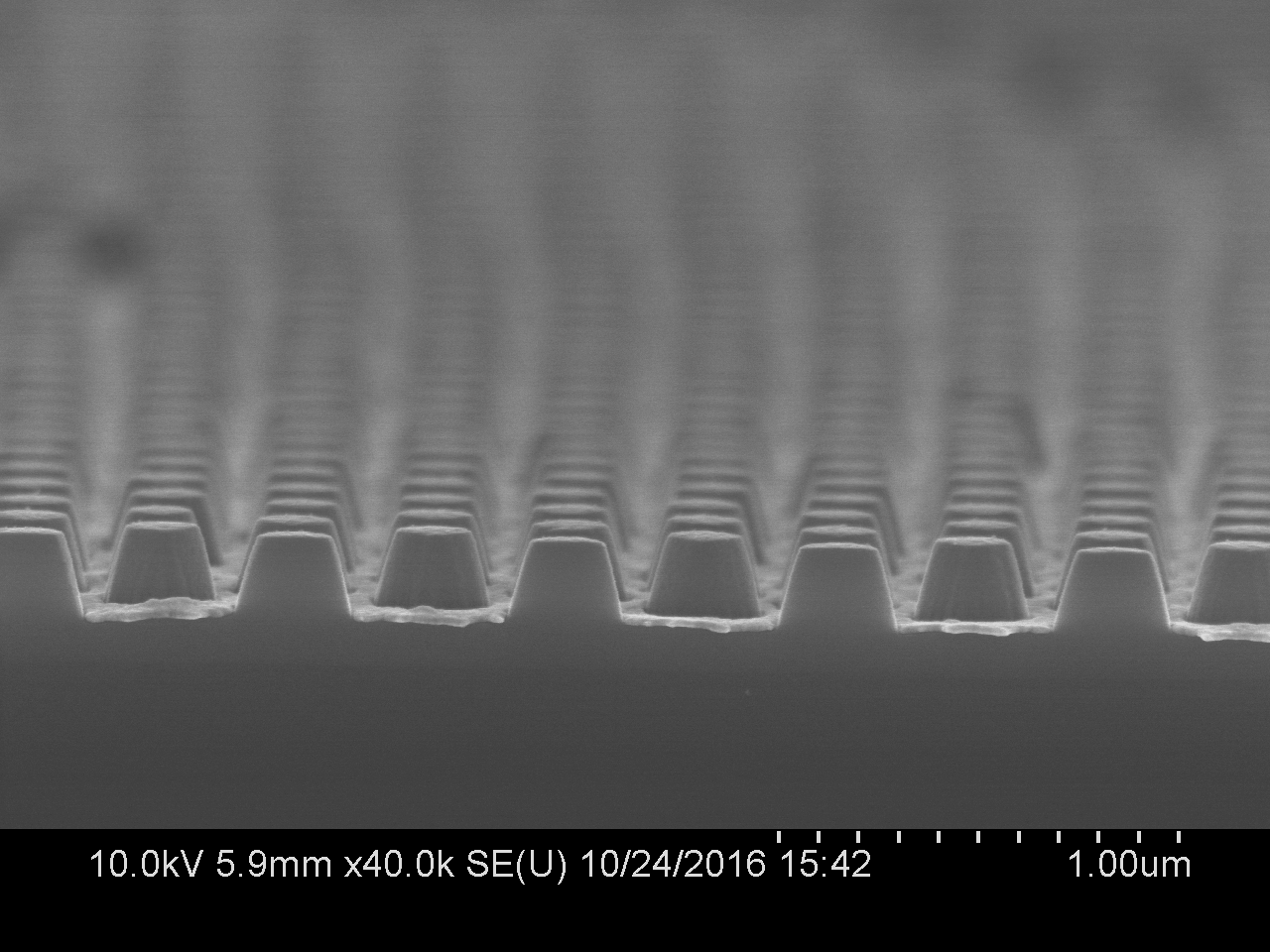
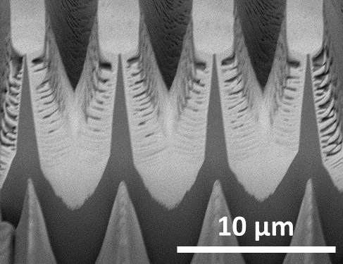
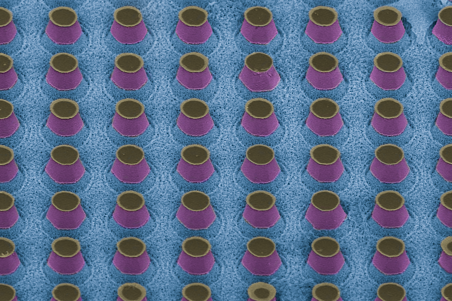
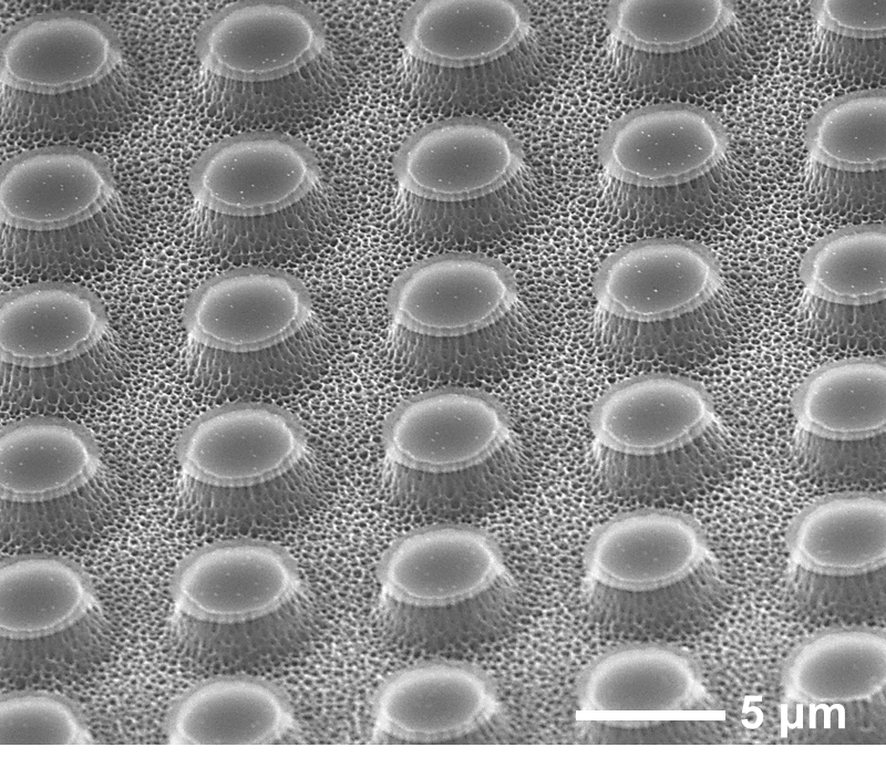
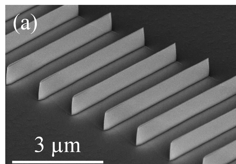
Selected micro- and nanostructures from published MacEtch studies.
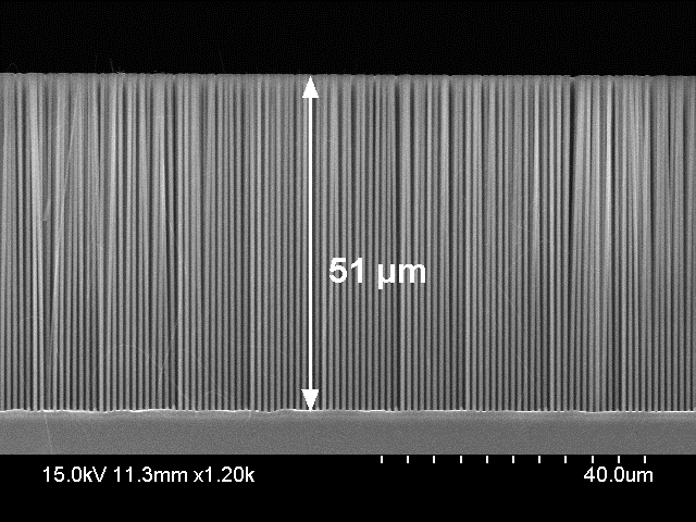
51-µm high-aspect-ratio structures
Translation
The MacEtch patent portfolio spans foundational chemistry, materials expansion, catalyst control, vapor-phase processing, optical surfaces, monolithic microLED fabrication, and radiation-enabled systems.
Explore the MacEtch patent portfolio →Porous silicon and porous III–V formation
3D patterns and high-aspect-ratio arrays
Magnetic guidance, self-anchoring, vapor phase
Optoelectronics, microLEDs, and radiation-enabled systems
The broader opportunity
It is positioned to potentially revolutionize the traditional RIE approach across diverse fields such as electronics, photonics, quantum, energy, and bio-sensing applications.